國立台灣大學林清富教授實驗室
研究領域摘要
主題二:晶體型半導體薄膜太陽能電池
研究人員: 趙俊傑
英文摘要:
Because of the significant increase of petroleum and greenhouse effect caused by the carbon dioxide generated from the burning carbon-related fuel, there is an
urgent need of using alternative energy, in particular, the renewable energy sources. Among those renewable energy sources, using solar energy is the most
attractive for its abundant supply form the sun and clean, no pollution characteristics. However, current solar cells are mainly made from bulk Si or bulk III-V
semiconductors. Unfortunately, those types of solar cells need large amount of raw materials, causing the high cost of production. Thus thin-film solar cells are
regarded as good solutions to reduce the material usage.
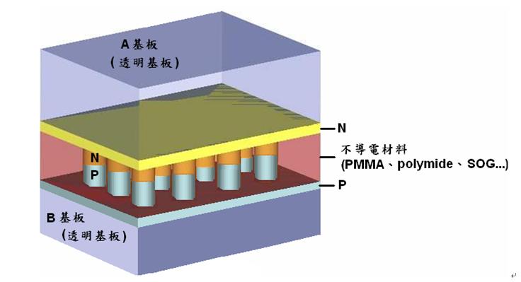
We propose a novel technique to develop crystalline semiconductor thin-film solar cells. As shown in Fig. 1, the concept is to transfer crystalline Si nano/micro-
structure or III-V compound nano/micro-structure onto alien substrates to fabricate solar cells without lattice-matched concern. This thin-film solar cell with high
crystal quality presents high power conversion efficiency. Besides, the thin-film type offers the advantages of large-area fabrication and the bending flexibility.
Fig. 1 the conceptual structure of crystalline semiconductor thin-film solar cells
The following is the transfer technique we have developed. InGaP/GaAs double-junction square-based (25μm×25μm) micro-cuboid arrays were released from
GaAs substrate by the epitaxial lift-off process. These InGaP/GaAs micro-cuboid arrays were transplanted to the P3HT film spun on ITO glass substrate
successfully. Besides the significant cost reduction, our method shows the rapid transplantation and the potential for high-efficiency large-area devices
fabrication.
As a result of the ability to tune the band-gap of III-V compound semiconductor materials to match the solar spectrum, solar cells made from these materials
have unsurpassed conversion efficiencies. The most frequently used materials for III–V solar cells such as GaAs and InGaP are direct band gap
semiconductors with high absorption coefficients. A stack with a thickness of only a few micrometers of these materials is required to absorb all light that the
cell can convert into electricity. However, III–V solar cells are usually not referred to as thin-film cells. The reason why III–V cells are not referred to as thin-
film, is that the cell structures are generally deposited on an approximately hundred-μm-thick GaAs or Ge wafer in order to obtain single crystal solar cell
structures.
However, after the deposition of the solar cell film, the substrate is of no further use for its performance. The reduction of the costs of III–V semiconductor
materials and an increase of the power to weight ratio is highly desired. The most successful method to achieve these goals is epitaxial lift-off (ELO). This
method uses a very thin (5-50nm) sacrificial AlxGa1-xAs (x>0.6) release layer which is grown between the device and the GaAs substrate. The thin film device
is released from its host substrate by selective etching of the AlxGa1-xAs release layer with aqueous HF solution, together with the compressive strain induced
by a wax layer. Owing to the large selectivity (>106) of the HF solution for etching of AlGaAs over GaAs, the original substrate is not affected and can be
reused.
A high lateral etch rate is considered essential for industrial applications for ELO technique. Therefore, recently lateral etch rate as obtained by different
approaches of the ELO method has been elaborated in literature, including preparing the samples with wax and submerging them in the HF solution until the
thin films were found floating in the solution after several hours or up to several days, the weight-induced ELO process (WI-ELO), and ELO with a stabilized
radius of curvature by guiding the temporary flexible carrier over a cylinder surface. A disadvantage of the weight-induced ELO process is that the flexible
carrier easily bends too much. This will results in cracking of the epitaxial layer structure. For this reason, the ELO process with a stabilized radius of curvature
by guiding the temporary flexible carrier over a cylinder surface was developed. For the above-mentioned approaches, the larger area of the lifted off epi-film,
the longer time of the ELO etching process and the greater risk of microscopic cleavage cracks. In order to shorten the ELO etching time and prevent the
microscopic cleavage cracks, we develop a unique transplantation method.
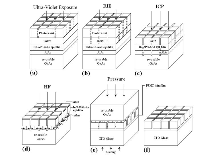
Fig. 2 Sequence of our experimental procedures
Fig. 2 shows the sequence of our experimental procedures. Before growing the InGaP/GaAs double-junction photovoltaic epi-film on the thick GaAs mother
substrate, thin sacrificial AlAs release layer were grown. After the epi-film growth, thick silicon dioxide (SiO2) layer was grown by PECVD. Afterward photo
resist was spun on SiO2 layer and proceed with UV photolithography as shown in Fig. 2(a). The size of each small cubic in the periodic patterns is
25μm×25μm. After photolithography, the patterns were transferred into the SiO2 layer coated on double-junction device by reactive ion etching (RIE) as
shown in Fig. 2(b) and then the photoresist was removed. The etching time was optimized to ensure a reliable pattern transfer, and at the same time to cause the
minimum damage to the surface of double-junction device. After the RIE etching, the periodic square-based (25μm×25μm) patterns were precisely transferred
to the SiO2 mask template as shown in Fig. 3, with a slight increase of the linewidth less than 5%.
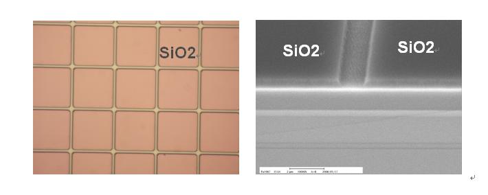
Fig. 3 transfer the periodic cubic patterns into SiO2 layer coated on InGaP/GaAs epi-film
The following procedure is opening a channel down to the sacrificial AlAs release layer by inductive coupled plasma (ICP) etching system as shown in Fig. 4(a)
The ICP etch time was also optimized to ensure the minimum damage to the surface of double-junction device beneath SiO2 mask. After the ICP etching,
the periodic square-based micro-cuboid arrays were accomplished as shown in Fig. 4(b).
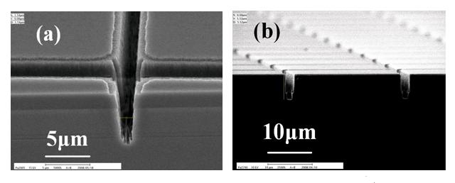
Fig. 4 InGaP/GaAs square-based micro-cuboid arrays. (a) Slots etched by ICP process, (b) Square-based micro-cuboid arrays
Then the sample was submerged in the aqueous HF solution to etch the sacrificial AlAs layer and the remaining SiO2 mask template after ICP etching as shown
in Fig. 2(d). The ELO submerged time must be shorter than the etch time required to completely release the epi-film from the GaAs substrate. After the rapid wet
etching of AlAs layer, there were very tiny AlAs which can remain beneath each cuboid. This tiny AlAs not only fixed each cuboid on GaAs substrate but also
can be snapped easily, as shown in Fig. 5.
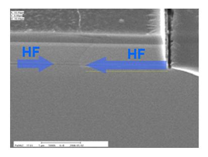
Fig. 5 After ELO, there were very tiny AlAs which can remain beneath each InGaP/GaAs cuboid
The square-based micro-cuboid arrays fabricated above were then transferred to a foreign receiver substrate. The transfer procedure is illustrated in Fig. 2(e).
The receiver substrate was first coated with P3HT [poly (3-hexylthiophene)]. Next, the P3HT was heated. The GaAs wafer with the square-based micro-cuboid
arrays was then pressed against the ITO glass and held there. In the meantime, the micro-cuboid arrays were stuck on the P3HT thin film. Then, the whole setup
was cooled down to room temperature. Various pressures were experimented. Finally, the GaAs host substrate was detached from the ITO glass. After the above
steps, the micro-cuboid arrays were transferred onto the ITO glass as shown in Fig. 6.
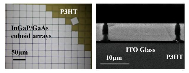
Fig. 6 the images after transferring InGaP/GaAs square-based micro-cuboid arrays on to ITO glass
(Left: top-view, right: cross-section)
We have successfully transferred InGaP/GaAs double-junction square-based (25μm×25μm) micro-cuboid photovoltaic arrays onto the P3HT film spun on
ITO glass substrate using the epitaxial lift-off (ELO) technique. Comparing with the conventional ELO method, including WI-ELO and ELO with a stabilized
radius of curvature, our new method shortens the lifted-off time greatly. Besides, for the above-mentioned approaches, when the area of the lifted off epi-film
becomes larger or the application of the device becomes more bending, the microscopic cleavage cracks may occur. This will limit its application and
performance. However, our new method shows the rapid transplantation and the potential for large-area devices fabrication simultaneously without the cracking
concern. It is expected that a large variety of substrates and much larger area of III-V thin film photovoltaic devices can be used for versatile applications in the
future.
中文摘要:
由於石油價格高漲及石化原料燃燒造成的溫室效應,替代性能源有急迫性的需要,其中太陽能發電是最受矚目的替代性能源。但由於目前太陽
能電池使用矽塊材及III-V族半導體,耗費材料太多,使得成本極高,因此薄膜型太陽能電池被認為是未來的解決方案。
此計畫提出一種創新概念,將發展一套轉移技術用以開發晶體型態的薄膜太陽能元件,如圖一所示,運用的材料包含了目前最常見的矽材料及
高效率光電特性的III-V族材料,主要優勢為克服了基板晶格常數配合的問題,以轉移方式將晶體型態薄膜轉移至各類合適的異質基板上製成太
陽能元件。此型薄膜太陽能電池由結晶良好的晶片蝕刻而得,使得元件保持了原有的良好晶體半導體特性,轉移技術更節省大量的材料成本並
提供了大面積及可撓之前瞻性。
圖一 晶體型半導體薄膜太陽能元件之構想結構
目前我們所發展出來的轉移技術詳述於下,先利用ELO (epitaxial lift-off)技術將InGaP/GaAs雙接面正方形(25μm×25μm)微米柱陣列從GaAs成長基
板上脫離,而後成功轉移至懸塗於ITO透明導電玻璃的P3HT[poly (3-hexylthiophene)]有機薄膜上。此轉移技術除了節省了大量昂貴的基板材料成
本,更具加速製程速度、大面積製作超高效率元件之潛力。
III-V族化合物材料提供了大範圍能階設計的誘人選擇,藉由選擇最佳能隙的半導體材料,以對應於每一個光頻譜範圍,使整體太陽光頻譜得到
最佳使用,最常用來製作III-V族太陽能電池的材料包含了像GaAs、InGaP等具高吸收係數的直接能隙材料。使用串聯堆疊結構,調變接面之能隙
使元件具有更廣大的吸收波長範圍,堆疊結構只需數微米就足以吸收大部分的太陽光頻譜並轉換成電能。然而,III-V族太陽能電池由於磊晶時
晶格常數上的匹配需要,往往須成長於厚度約為幾百微米的GaAs或Ge基板上,因此很少被視為薄膜太陽能電池。
然而,在成長完太陽能電池之串聯堆疊結構薄膜後,成長基板對於太陽能電池效率的表現上並沒有其他功能。因此,移除基板以節省基板材料
成本、同時增加功率對重量比有其需要,其中最成功的技術為ELO (epitaxial lift-off)技術。此技術首先於III-V族多接面磊晶層元件與磊晶成長的基
板間成長一層相當薄(5-50nm)的AlxGa1-xAs (x>0.6)犧牲層(sacrificial layer),蝕刻液為氫氟酸水溶液,主要原理為氫氟酸水溶液對於AlGaAs與
GaAs兩種材料蝕刻情形有相當大的選擇比(>106),藉由選擇性濕蝕刻的方式使III-V族多接面磊晶層元件脫離原本的砷化鎵成長基板,同時,砷化
鎵成長基板將不受影響而仍可重複使用。
側向蝕刻速率在ELO技術的應用上是非常重要的,目前已經有許多ELO技術被發展出來,而其對應的側向蝕刻也同時被報導,包含了:傳統作法
以蠟固定住元件結構再浸泡於氫氟酸水溶液中等待蝕刻完畢而浮起,其過程相當耗時,蝕刻時間往往長達數小時至數天,而後更發展出藉由重
物懸吊式ELO作法(WI-ELO;weight-induced ELO process)及滾輪式ELO作法(ELO with a stabilized radius of curvature)以加速其ELO製程時間,由於懸
吊式ELO容易使元件薄膜過度彎曲而造成微觀的裂縫瑕疵,進而影響到元件品質,因此發展出滾輪式ELO以固定元件薄膜的曲率。然而,對於以
上的ELO作法,由於為單方向蝕刻,導致大面積元件的移除相當耗時,同時在處理大面積轉移時,元件很容易發生微觀的裂縫瑕疵,進而影響
到元件品質。為了加速ELO蝕刻過程並排除微觀裂縫瑕疵的產生機會,我們發展了一種全新的轉移作法。
圖二 構想元件實行流程示意圖
其做法將詳述於下(見圖二): 首先在InGaP/GaAs雙接面磊晶層之太陽能薄膜元件及砷化鎵成長基板間成長一層AlAs犧牲層,以作為ELO (epitaxial
lift-off)之選擇性蝕刻使用。之後在薄膜元件上以PECVD成長一層SiO2層,再以微影技術將圖案化的光阻做為遮罩,如圖二(a)所示,其形狀為正
方形陣列遮罩,正方形之尺寸約為25μm×25μm,接著將此正方形陣列圖案利用RIE乾蝕刻機台轉印至SiO2層,如圖二(b)所示,最後將光阻移除
。對於RIE步驟而言,其蝕刻時間必須精確控制,使得正方形陣列圖案能準確的轉印至SiO2層,同時能不影響到薄膜元件表面。對於此步驟的結
果,如圖三所示,正方形陣列圖案已能準確的轉印至SiO2層,同時正方形間之間距線寬約略增加在5%以下。
圖三 利用RIE乾蝕刻機台將正方形陣列圖案轉印至InGaP/GaAs磊晶層上的SiO2層
接下來的步驟為使用ICP乾蝕刻機台蝕刻InGaP/GaAs雙接面磊晶層,以製作出溝槽深度至AlAs犧牲層的溝槽,如圖四(a)所示,其蝕刻時間也是必
須精確控制,使其不影響到薄膜元件表面,此時,InGaP/GaAs雙接面磊晶層將成為正方面體陣列,如圖四(b)所示。
圖四 InGaP/GaAs正方面體微米陣列 (a) 以ICP乾蝕刻機台製作出溝槽 (b) 正方面體微米陣列
之後進行ELO蝕刻步驟,將磊晶層基板浸泡於氫氟酸水溶液中,如圖二(d)所示,蝕刻時間應略短於AlAs犧牲層完全蝕刻殆盡之前,使得每個正
方面體下方剩下一根相當細小的AlAs柱狀,讓每個正方面體還能固定於基板之上,同時此細小的AlAs柱也很容易將其折斷,如圖五所示。
圖五 經過ELO後,InGaP/GaAs正方面體下方剩下部份的AlAs柱狀
接著,將正方面體微米陣列轉移至異質接載基板上,如圖二(e)所示。此處所使用的異質接載基板為ITO透明導電玻璃,首先在ITO玻璃上懸塗上
P3HT有機薄膜,而後將具正方面體微米陣列之磊晶基板倒置並熱壓於上,待冷卻固化至室溫,此時正方面體微米陣列已黏至該ITO玻璃上。最
後,將原GaAs成長基板移除,成功地將正方面體微米陣列轉移至ITO玻璃上,如圖六所示。
圖六 將InGaP/GaAs正方面體微米陣列轉移至ITO玻璃上之P3HT有機薄膜 (左:俯視圖;右:側面圖)
我們已經成功利用ELO技術轉移InGaP/GaAs正方面體(25μm×25μm)微米陣列轉移至ITO玻璃上之P3HT有機薄膜。相較於其他ELO轉移技術的最
大優點在於,由於ELO技術側向蝕刻速率並不高,若採取一般ELO作法由單方向開始蝕刻,過程過長,導致大面積元件的轉移相當耗時,蝕刻時
間往往長達數小時至數天,蝕刻速率較快的重物懸吊式ELO作法或是滾輪式ELO作法在處理大面積轉移時,元件很容易發生微觀的裂縫瑕疵,進
而影響到元件品質,同時上述兩種ELO作法仍為單方向蝕刻,所以過程仍相當耗時。我們的作法除了ELO蝕刻過程相當迅速,而且排除了微觀裂
縫瑕疵的產生機會,對於在III-V族薄膜型太陽能電池的應用上,以期有大面積製作、同時壓低成本、轉移於適合基板(甚至提供可撓之可能性)、
加速製程速度等應用潛力。
最新消息 研究領域摘要 指導教授 研究計畫 報帳資訊 實驗室成員 相關連結 回首頁